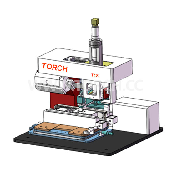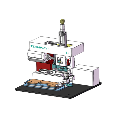
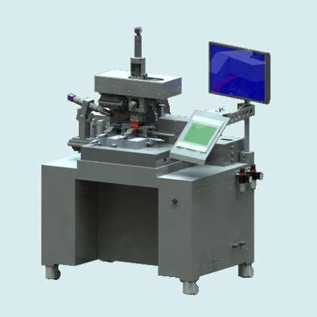
Die Bonder T1
- Product Description
T1 is a multi-functional mounter, which can provide up to 5 μ m precision. It is suitable for mounting all kinds of flip chip and ordinary chip, and can handle chip spacing as low as 50 μ M. This universal placement platform is suitable for a wide range of micro assembly applications, covering a lot of micro assembly process, and even can be configured as FC / SMD repair system.
It is mainly designed for medium and small batch production, as well as to meet the needs of prototype manufacturing, scientific research and development, university teaching and research and other fields.
Application:
1. Flip chip bonding (face down).
2. High precision chip bonding (face up).
3. Laser diode, laser bar welding.
4. VCSEL, PD, lens package.
5. LED packaging.
6. Micro optical device packaging.
7. MEMS packaging.
8. Sensor package.
9. 3D Packaging.
10. Wafer level package (W2W, c2w).
11. Chip to glass substrate, chip to flexible substrate mounting.
Standard configuration:
1. Hot pressing.
2. Thermal ultrasound.
3. Ultrasound.
4. Reflow and sintering (AU Sn, C4, in, eutectic).
5. Adhesive process.
6. Curing (UV, temperature).
7. Mechanical assembly.
Highlights:
1. Mounting accuracy: better than 5 μ M.
2. Element size: 0.125 mm x 0.125 mm- 100 mm x 100 mm* 100 mm x 100 mm* .
3. Maximum working area: 450 mm x 122 mm* .
4. Support maximum wafer size: 8 " .
5. Maximum mounting pressure: 700 n*.
6. It can be configured as hot air repair system.
7. Manual and semi-automatic distribution.
Features:
1. Automatic process and data processing.
2. Spectrometer vision alignment system.
3. Process integration and process management.
4. Real time process observation camera.
5. Intelligent system software and adaptive program librar.y
6. General transfer of process procedures between different systems, covering many interconnected processes.
7. Modular design, strong process flexibility.
Advantages:
1. The multi-function high-precision Mounter has no manual chip mounting, which eliminates the influence of personnel factors.
2. Superior mounting accuracy, ready to use, no need to adjust.
3. Realize the synchronous control of all process parameters: pressure, temperature, time, power, process environment, lighting and video.
4. Real time observation and feedback greatly shorten the process development time.
5. The process development is simple and convenient, supporting the automatic recording of the process.
6. Quickly transform R & D process to production process.
7. One platform can realize many process applications.
Technical parameters:
1. Field of view (minimum): 1.6mm * 1.2mm.
2. Field of view (maximum): 20mm * 15mm.
3. Element size (minimum): 0.125mm * 0.125mm.
4. Fine adjustment of Φ axis: ± 6 degree
5. Z-axis stroke of worktable: 10mm.
6. Working area: 280mm * 117mm.
7. Heating temperature (maximum) 400 ℃
8. Mounting pressure (maximum) 700n.
Modules and options:
1. ACF module.
2. Ball planting module.
3. Chip force control module (automatic).
4. Chip heating module.
5. Blue film taking module.
6. Camera mobile module.
7. Inert gas protection module.
8. Process video observation module.
9. Friction module.
10. Substrate heating module.